Connector Surfaces – Influence on PIM
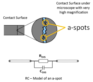
New connector surfaces look and feel very smooth, but the picture changes quickly when viewed under a microscope. The atomic lattice size of metals is often no more than 25 Angstroms (0.0000025 mm) wide. Machined metal surfaces will never have such a degree of smoothness. Metallic surfaces look indeed very rough under high magnification. That causes surfaces of mated connectors to touch only at a few spots,  called asperities. Tightening connectors applies localized pressure to these asperities, which causes them to deform. Deformations increases the contact area, but it is still limited to some “load-bearing” areas, so called a-spots. They add up, but their overall area is still by several orders of magnitude smaller than the apparent contact surface of connectors.
Lengths of the constrictions are very short, so inductive effects are small compared to capacitive and resistive effects. Simplified, a-spots can be regarded as electrical RC models and a mated connector can be seen as network of thousands of unequal RC circuits. Such a network does not behave in a linear way. Passing currents of different frequencies will respond differently. This causes passive intermodulation. Structural material discontinuity causes also discontinuity in current flow. Regardless of the contact material, discontinuity in electron flow is characterized by:
- Constriction Resistance – due to bending of current lines of flow in the vicinity of an a-spot.
- Tunnel Resistance – due to conduction through thin insulating contaminant layers via tunnel effect.
- Contact Capacitance – between the two essentially parallel equipotential surfaces.
Skin Effect
 Skin effect is called the property of alternating current to show higher current density closer to a conductor surface. Current flows mainly at the “skin” of the conductor between the outer surface and a level called the skin depth. Skin effect is caused by eddy currents that are induced by the changing magnetic field of alternating current.
The effect is more pronounced with higher frequencies. At 1 GHz, on a silver plated surface, around 98 % of the current density occurs within approximately 0.01 mm of material depth. For comparison: an average human hair has a diameter of 0.08 mm, 8 times larger in diameter than the skin depth at 1 GHz. This fact underlines the importance of connector plating. It serves not only as protection for the connector but carries almost all of the current in RF systems. The remarkably diminutive skin depth of conductors at high frequencies is very susceptible to scratches in the material. Even if only on a microscopic scale, the tiniest groove, dent or jag interferes with homogeneous flow of current and with that, causes unwanted passive intermodulation.
Subscribe for free technical publications from AWT Global


